Majorana, the third!
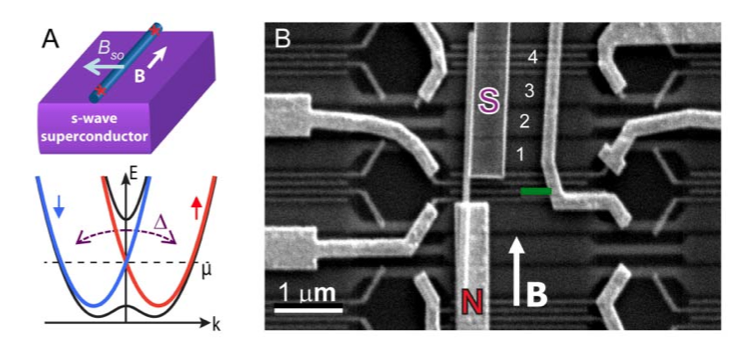
Last week, two groups reported the discovery of a pair of Majorana quasiparticles at the end of a semiconductor wire.
Their probe was the creation of zero energy level in the two ends of the wire. Applying bias current through the wire and measuring conductance of the wire in the lack and presence of magnetic field indicates: whenever the field above a limit is applied on the wire (perpendicular to internal spin-orbit moment), a "strange" zero energy levels appears. This energy level is firmly stuck on the zero energy (doesn't want to split or shift from zero a bit in stronger fields!) This is similar to what expected from Majorana quasiparticles.
Browsing arXiv shows one other experiment has been completed in similar setups (submitted 3 days before Kouwenhoven submit their initial work) in which a signature other than the zero energy level of these particles is experimented.
In this work, on the same setup as used now they applied an rf voltage on the wire and measured the IV plot. The Shappiro steps was observed. These steps were already known from the Josephson junction studies. When rf voltage applies on a Josephson junction the voltage causes phase difference in the junction to oscillate. When this is considered in the supercurrent-phase relation (i.e. I=sin(phase)), gives rise to some phase lock-ins at harmonics of the rf frequency. The amplitude of the beatings is sensitive to the power of the rf voltage. In other words, the average voltage jumps from one value to another by the increase of bas current through the wire.
The precise fact about these steps is that the size of the voltage steps is inversely proportional to the charge of carrier particles. If the carrier is of charge e' the step size is proportional to 1/e'. For instance, in a Josephson junction that the carriers are cooper pairs the step sizes are proportional to 1/(2*e).
Rokhinson, Liu and Furdyna in this paper show similar effect (instead of a Josephson junction, now) on the InSn nanowire in the setup used for observation of Majorana. Interestingly they observed without magnetic field the voltage steps are proportional to 1/(2*e). When they apply 2.7T along the wire they start to observe the size of the steps is doubled, which means in the new regime the carriers have the charge e instead of 2*e. Below, you see the doubling of the size of steps:
Although they found an interesting phenomenon, but in their supplementary material their fitting Bessel function seems not to be perfectly approved experimentally!
Nonetheless, The only concern is that the magnetic field required to create the Majororana in InSb is 100mT applied along the wire. In this experiment, they do not see the effect even at 20 times larger field and only started to observe the effective e-charge carrier at B~2.7T. Note that in 1T the zero bias voltage starts to split so it is likely the Majorna quasiparticles are mixed up with something else of the type of Kondo levels (look at the plot of "Fig.2" in here.)
Is this really due to Majorana quasiparticle? Maybe...
Last week, two groups reported the discovery of a pair of Majorana quasiparticles at the end of a semiconductor wire.
Their probe was the creation of zero energy level in the two ends of the wire. Applying bias current through the wire and measuring conductance of the wire in the lack and presence of magnetic field indicates: whenever the field above a limit is applied on the wire (perpendicular to internal spin-orbit moment), a "strange" zero energy levels appears. This energy level is firmly stuck on the zero energy (doesn't want to split or shift from zero a bit in stronger fields!) This is similar to what expected from Majorana quasiparticles.
Browsing arXiv shows one other experiment has been completed in similar setups (submitted 3 days before Kouwenhoven submit their initial work) in which a signature other than the zero energy level of these particles is experimented.
Here it is:
"Observation of the fractional ac Josephson effect: the signature of Majorana particles", by Leonid P. Rokhinson, Xinyu Liu, and Jacek K. Furdyna, arXiv:1204.4212
In this work, on the same setup as used now they applied an rf voltage on the wire and measured the IV plot. The Shappiro steps was observed. These steps were already known from the Josephson junction studies. When rf voltage applies on a Josephson junction the voltage causes phase difference in the junction to oscillate. When this is considered in the supercurrent-phase relation (i.e. I=sin(phase)), gives rise to some phase lock-ins at harmonics of the rf frequency. The amplitude of the beatings is sensitive to the power of the rf voltage. In other words, the average voltage jumps from one value to another by the increase of bas current through the wire.
The precise fact about these steps is that the size of the voltage steps is inversely proportional to the charge of carrier particles. If the carrier is of charge e' the step size is proportional to 1/e'. For instance, in a Josephson junction that the carriers are cooper pairs the step sizes are proportional to 1/(2*e).
Rokhinson, Liu and Furdyna in this paper show similar effect (instead of a Josephson junction, now) on the InSn nanowire in the setup used for observation of Majorana. Interestingly they observed without magnetic field the voltage steps are proportional to 1/(2*e). When they apply 2.7T along the wire they start to observe the size of the steps is doubled, which means in the new regime the carriers have the charge e instead of 2*e. Below, you see the doubling of the size of steps:
 |
| Fig1. The y-axis is the average voltage measured in the wire. Left graph shows in small magnetic field the steps are still proportional to the cooper pair charge, however when the wire is bring to higher magnetic field in which Majorana should appear the size of the steps is doubled which means the carrier of charge e are coherent at zero energy level. These new carrier are perhaps Majorana quasiparticles. |
Although they found an interesting phenomenon, but in their supplementary material their fitting Bessel function seems not to be perfectly approved experimentally!
Nonetheless, The only concern is that the magnetic field required to create the Majororana in InSb is 100mT applied along the wire. In this experiment, they do not see the effect even at 20 times larger field and only started to observe the effective e-charge carrier at B~2.7T. Note that in 1T the zero bias voltage starts to split so it is likely the Majorna quasiparticles are mixed up with something else of the type of Kondo levels (look at the plot of "Fig.2" in here.)
Is this really due to Majorana quasiparticle? Maybe...